Capabilities
- When we think about capabilities, we think about what our customers’ needs are. We want to be able to handle all of our customers’ needs both today and in the future.
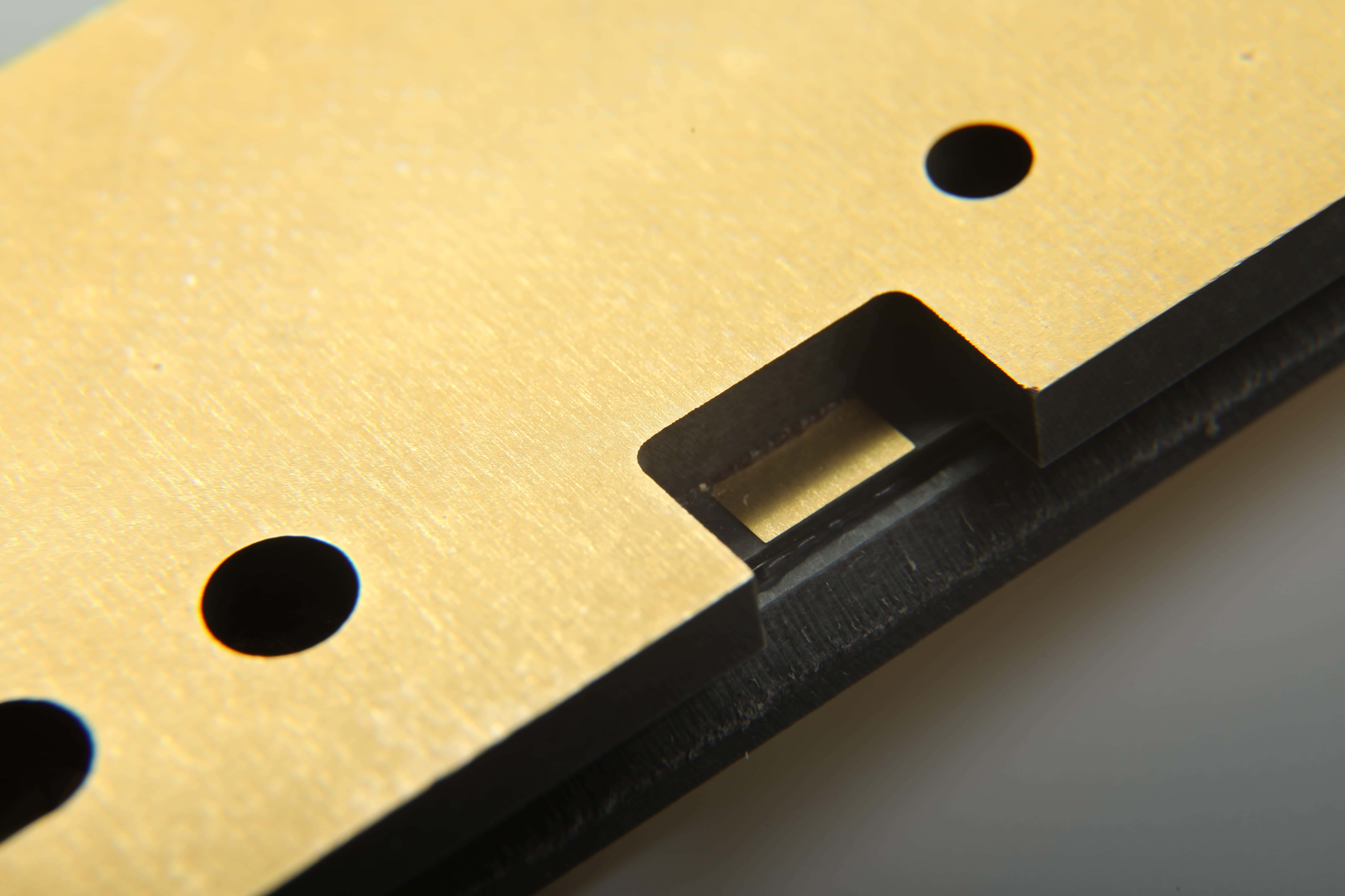
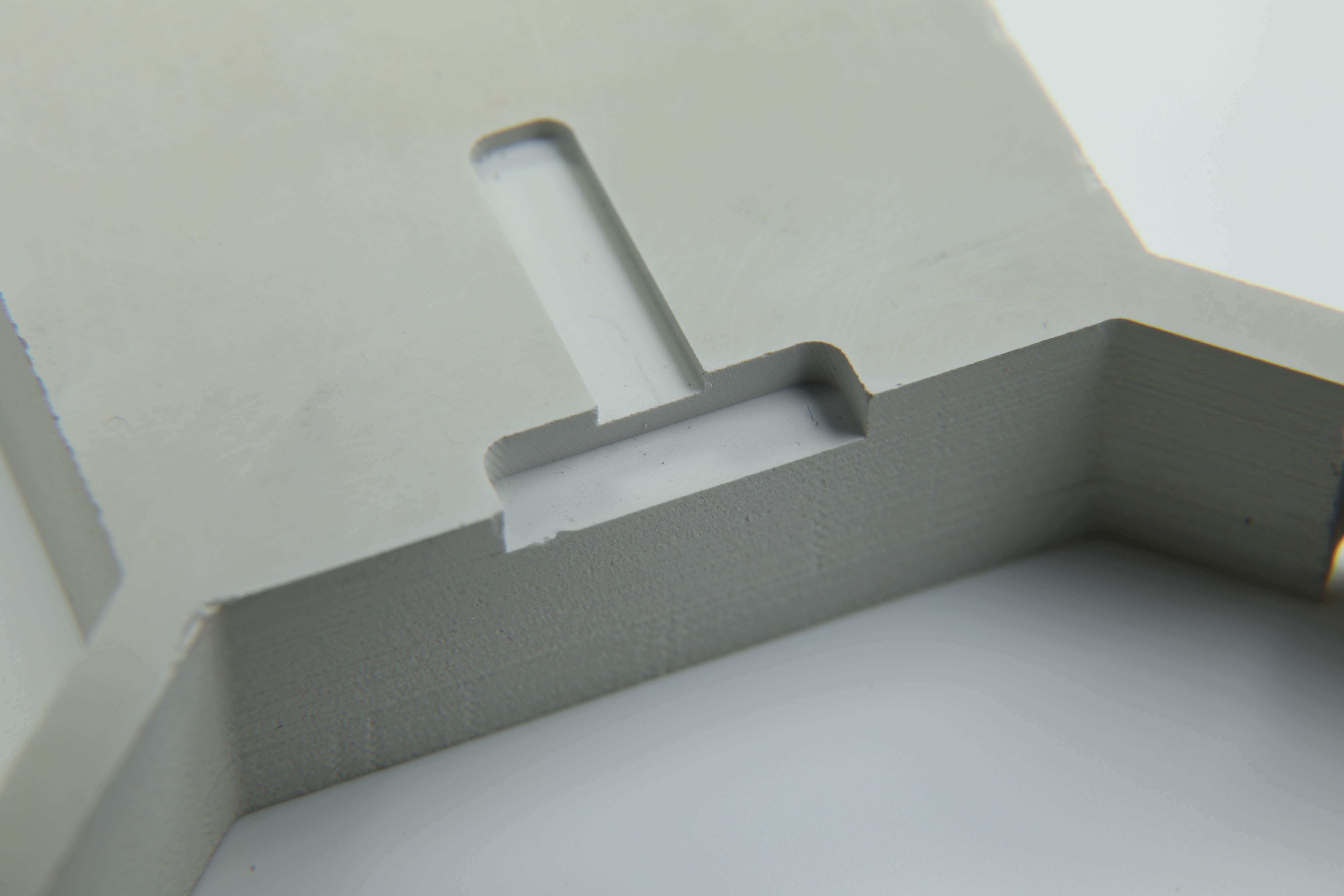
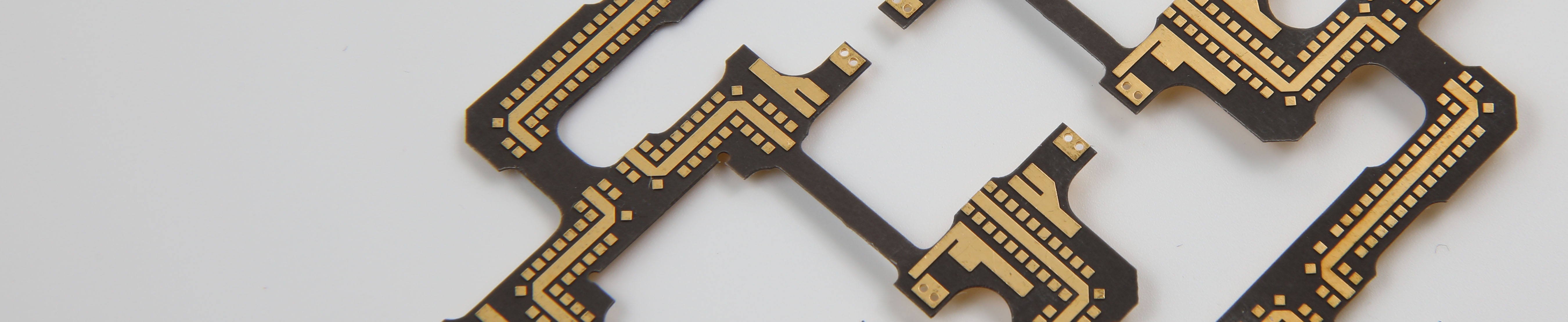
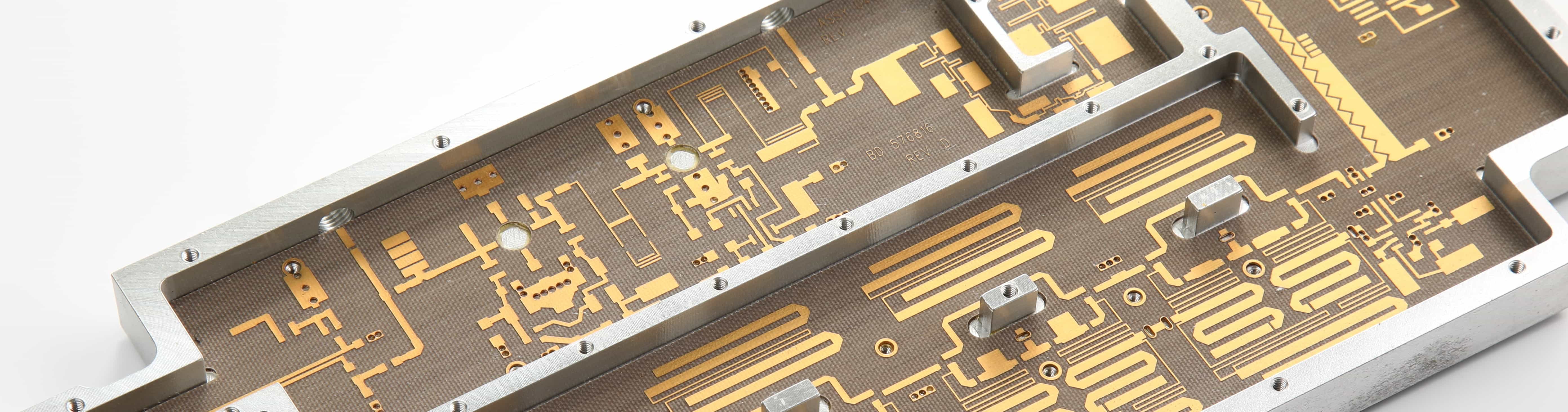
- Mega Circuit is considered one of the most capable PCB fabricators in the industry, from rigid to flex and rigid flex PCBs to Metal Core and heavy copper boards, from basic FR4 PCBs to high tech thermal PCBs using high tech thermal materials, we do it all.
- In fact, we are one of the few companies in the world that can build long PCBs up to 125 inches. Our goal is to be the most capable PCB fabricator in the industry.
-
Maximum Number of Layers
up to 36 layers
-
Minimum dielectric thickness
0.002"
-
Maximum Finished PCB Thickness
0.50"
-
Maximum Panel Size
24" x 125"
-
Outer Layers Finished Copper
maximum 11 oz
-
Inner Layers Finished Copper
maximum 11 oz
-
Plating in Holes
up to 10 oz
-
Minimum Outer Line Width
0.0025"
-
Minimum Inner Line Width
0.0025"
-
Minimum Space, PCB Edge to Conductor
0.005"
-
Clearance - Copper to the Center of Score-line
0.0012"
-
Clearance - Copper to Edge of Board
0.005"
-
Minimum component pitch
0.004"
-
Minimum Mechanical Drill Size
0.004"
-
Maximum Aspect Ratio
12:1
-
Hole to Hole Spacing
0.004"
-
Via Fill (Conductive & Non-conductive)
Yes
-
Blind/Buried Vias
Yes
-
Micro Vias/HDI
Yes
-
Stacked Vias
Yes
-
Back Drill
Yes
-
Minimum Router Bit Size
0.011"
-
Minimum Slot width
0.011"
-
Spacing for Tab Rout
0.031"
-
V-Score
Yes
-
Jump Score
Yes
-
Countersinks
Yes
-
Counterbores
Yes
-
Edge Castellations
Yes
-
Fabrication Radius
0.005"
-
Layer-to-Layer Registration
± 0.003"
-
Dimensions-Fab O.D.
± 0.005"
-
Plated Hole
± 0.002"
-
Non Plated Hole
± 0.001"
-
Fabrication/Rout
± 0.003"
-
Solder Mask Clearance Line Coverage
0.0025"
-
Minimum Solder Mask Dam
0.0035"
-
Tented Vias
Yes
-
Mask Plugged Vias
Yes
-
Peelable Solder Mask
Yes
-
Low Friction Solder Mask
Yes
-
LED Ultra White Solder Mask
Yes
-
Minimum Legend Width
0.005"
-
Space between Silkscreen & Pad
0.003"
-
TIN-LEAD HASL
Yes
-
Lead Free HASL
Yes
-
Immersion Silver
Yes
-
Organic Coverage (OSP)
Yes
-
Immersion Ni/Au Thickness
Ni 40-800 µinches Au 1-5 µinches
-
Hard Gold/Wire Bondable Soft Gold
Yes
-
ENEPIG
Yes
-
Immersion Tin
Yes
-
Gold Tabs
Yes
-
Impedance Tolerance
± 5%
-
TDR Testing
Yes