(a).jpg)
RF/Microwave
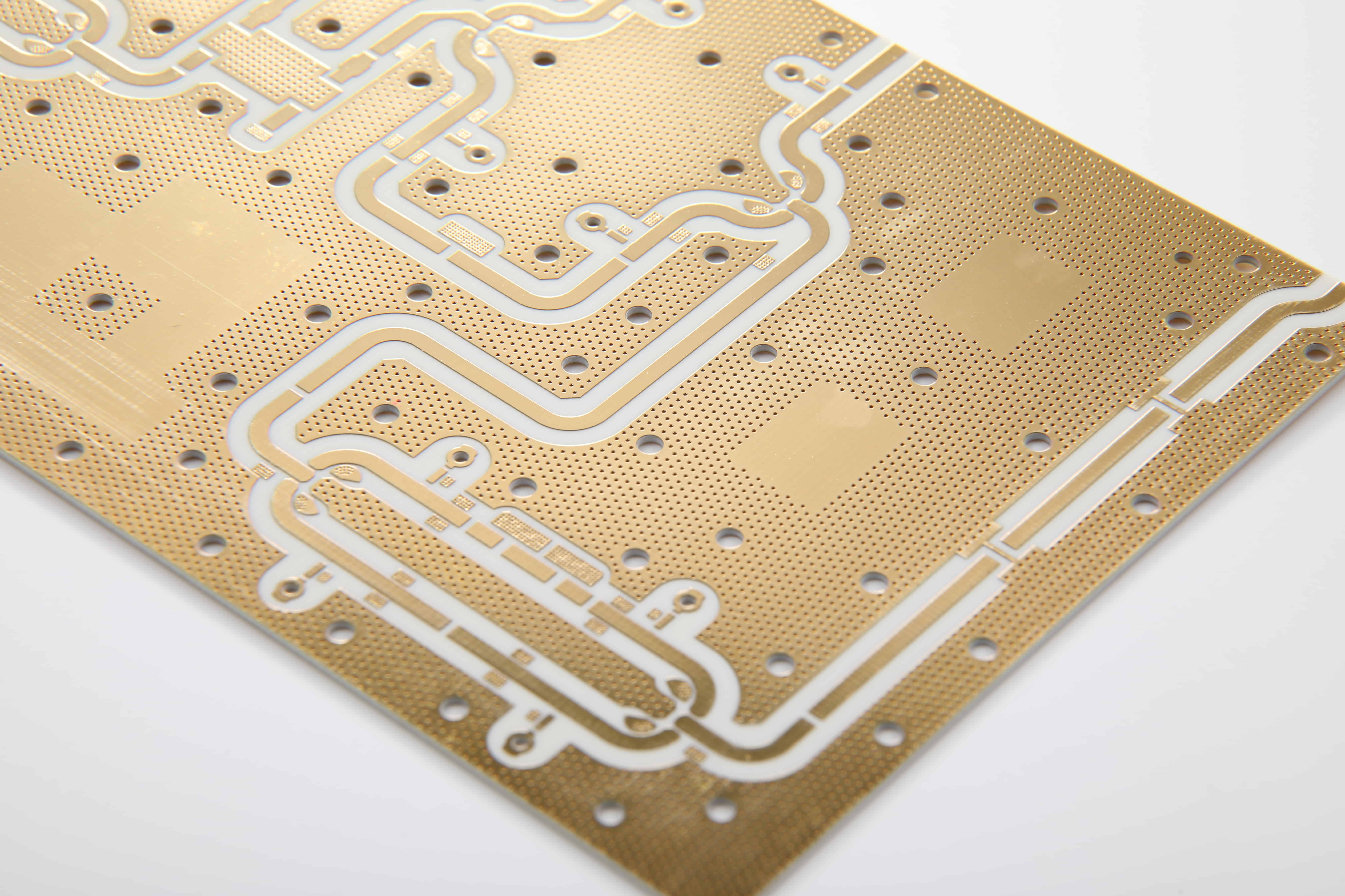
- Mega Circuit is a pioneer and world leader in the field of RF/Microwave PCB manufacturing.
- Our proprietary approach and experience make us uniquely successful serving critical performance-oriented markets.
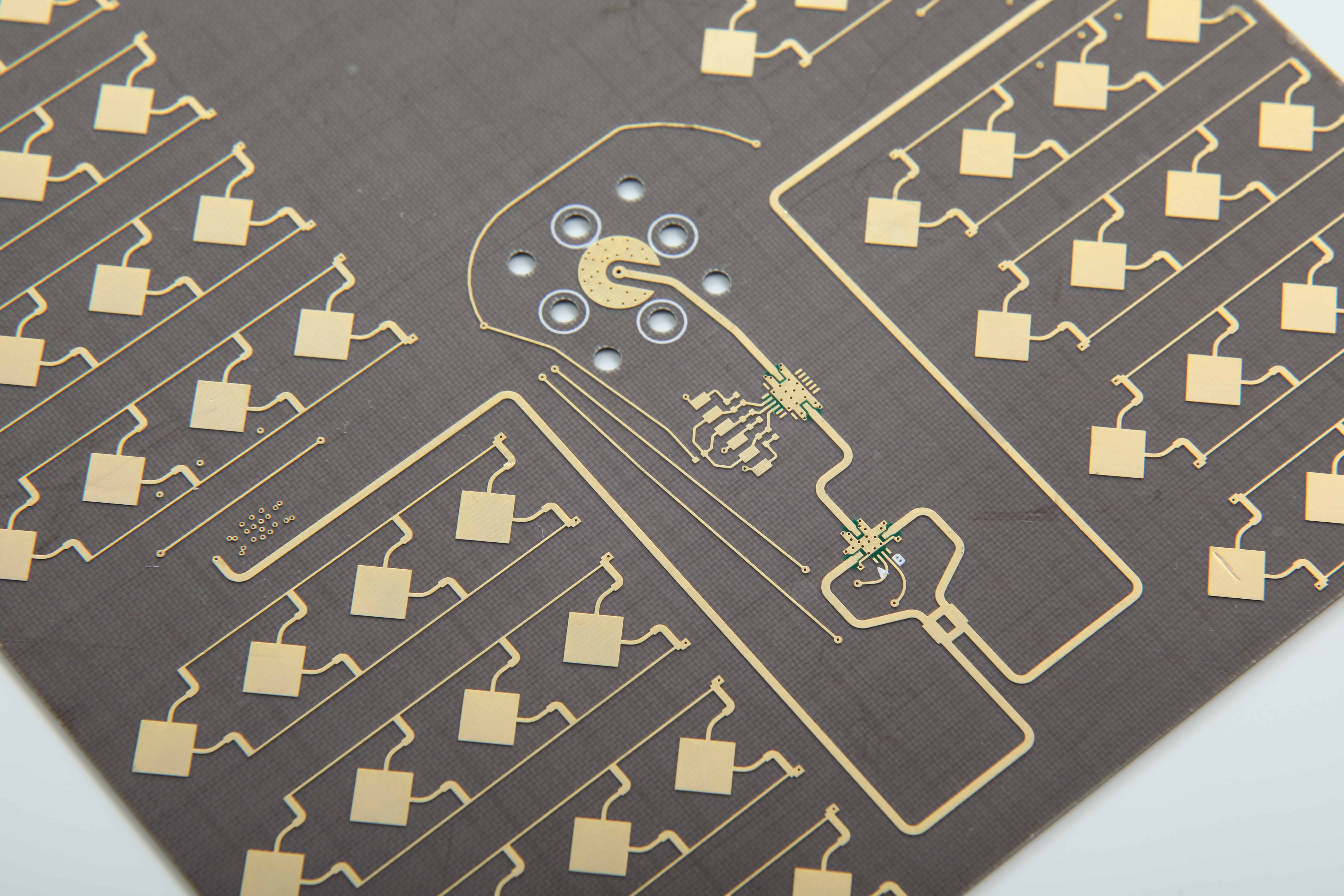
- We meet the challenges of our numerous customers with evolutionary requirements incorporating; PTFE, low loss Teflon laminates, hybrid as well as other exotic materials and constructions.
- From; Defense/Aerospace, Telecommunication, Medical Devices/Imaging to complex ever evolving RF/Microwave subsystems covering a vast spectrum of RF/Microwave frequencies, Mega Circuit has the experience and ingenuity to meet your technological and production challenges.
- At Mega, we understand the complexity of RF/Microwave PCB manufacturing as well as the competitive demands of this market. Our team's experience with a vast array of RF materials ensures your orders are designed for manufacturability, produced on time, and within budget.
Capabilities
Conductive & Nonconductive Via fill for all laminates > 0.01” thick.
Final finishes include ENIG, ENEPIG, Immersion Silver, Wire Bondable Gold, Hard & Soft Gold, Selective Gold Plating, HASL, Lead Free HASL, Immersion Tin, OSP and selective combinations
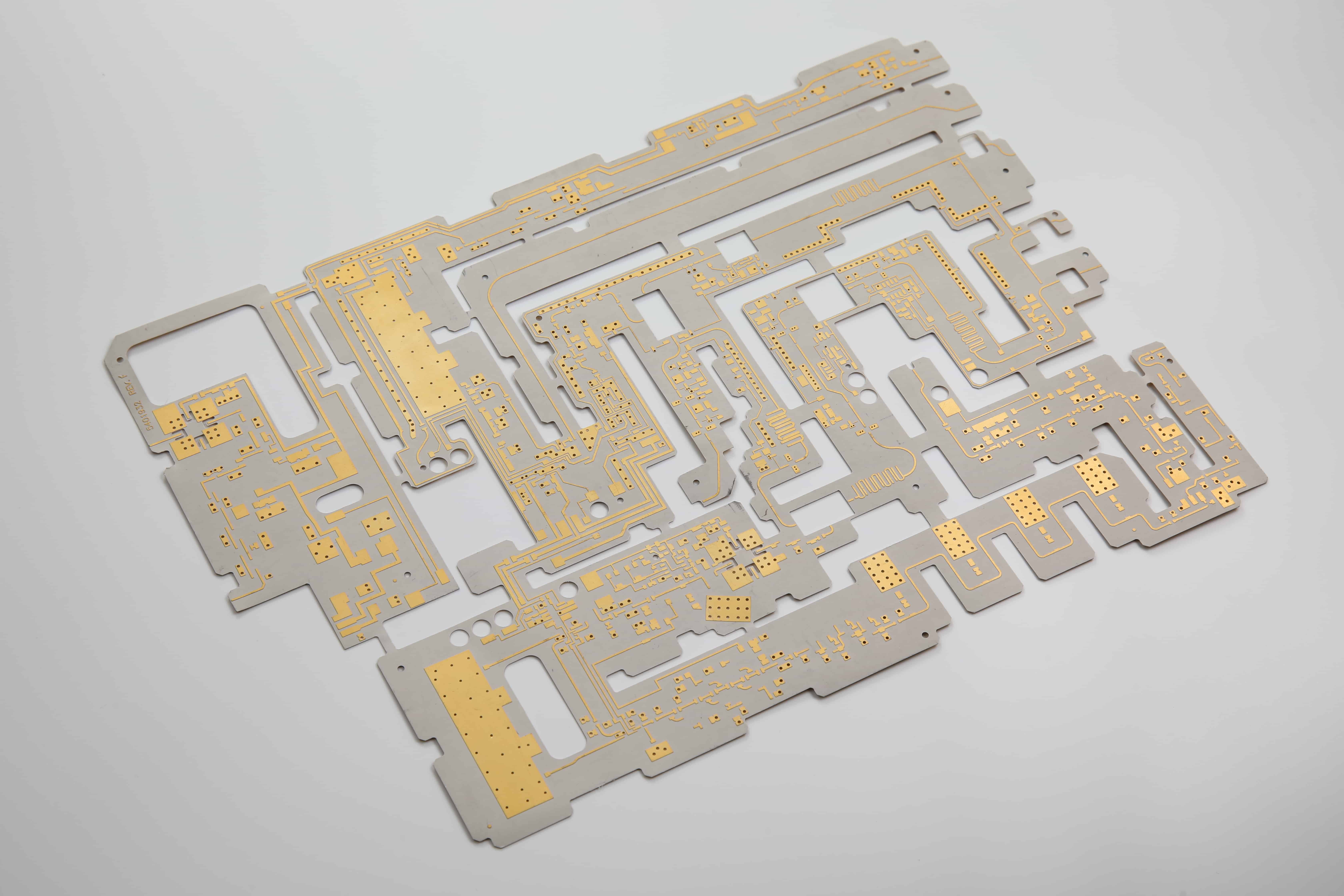
Blind & Buried Vias
Edge Plating & Castellations
Sequential Lamination
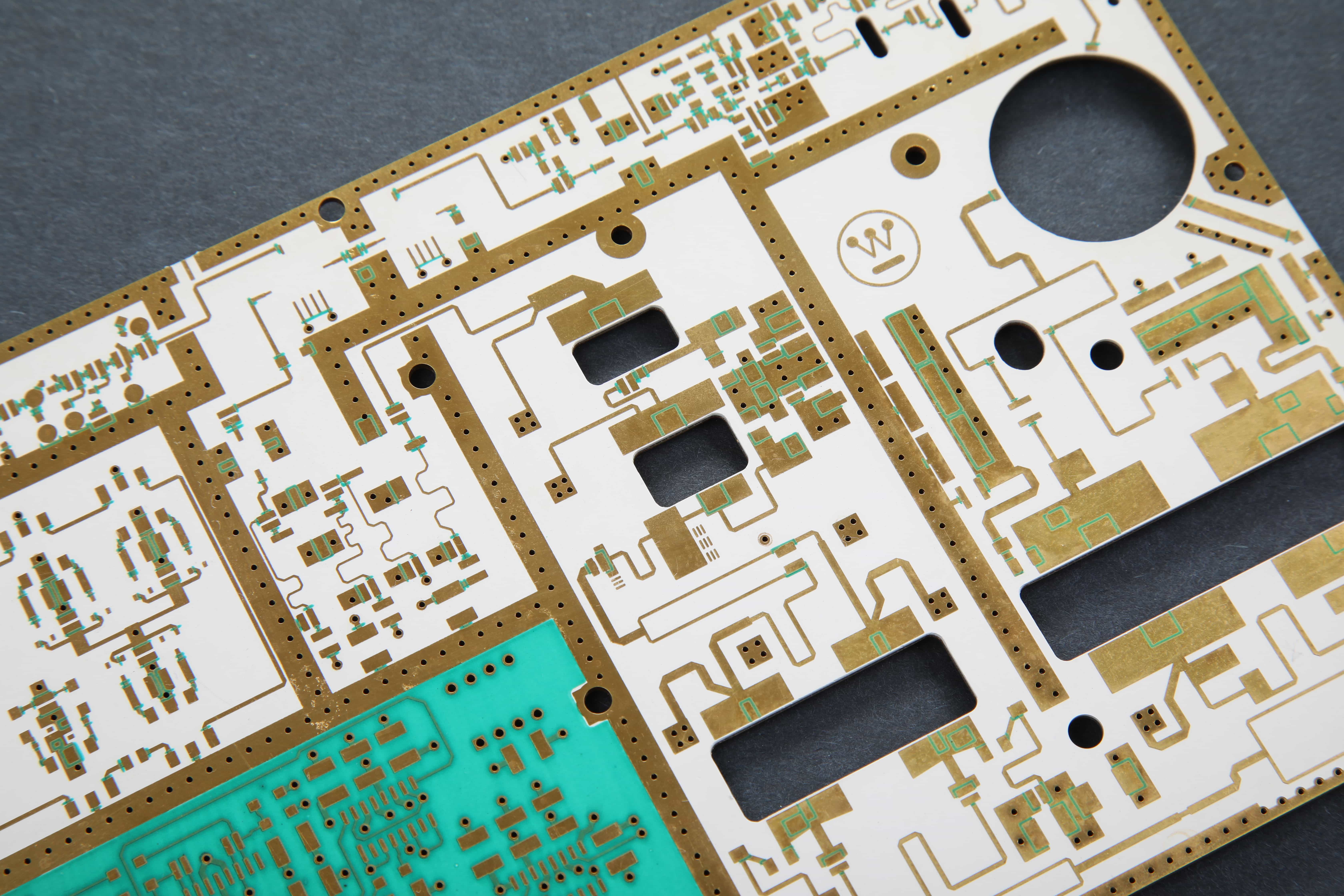
Cavities and Recessed Launch Sites
Hybrid multilayer constructions
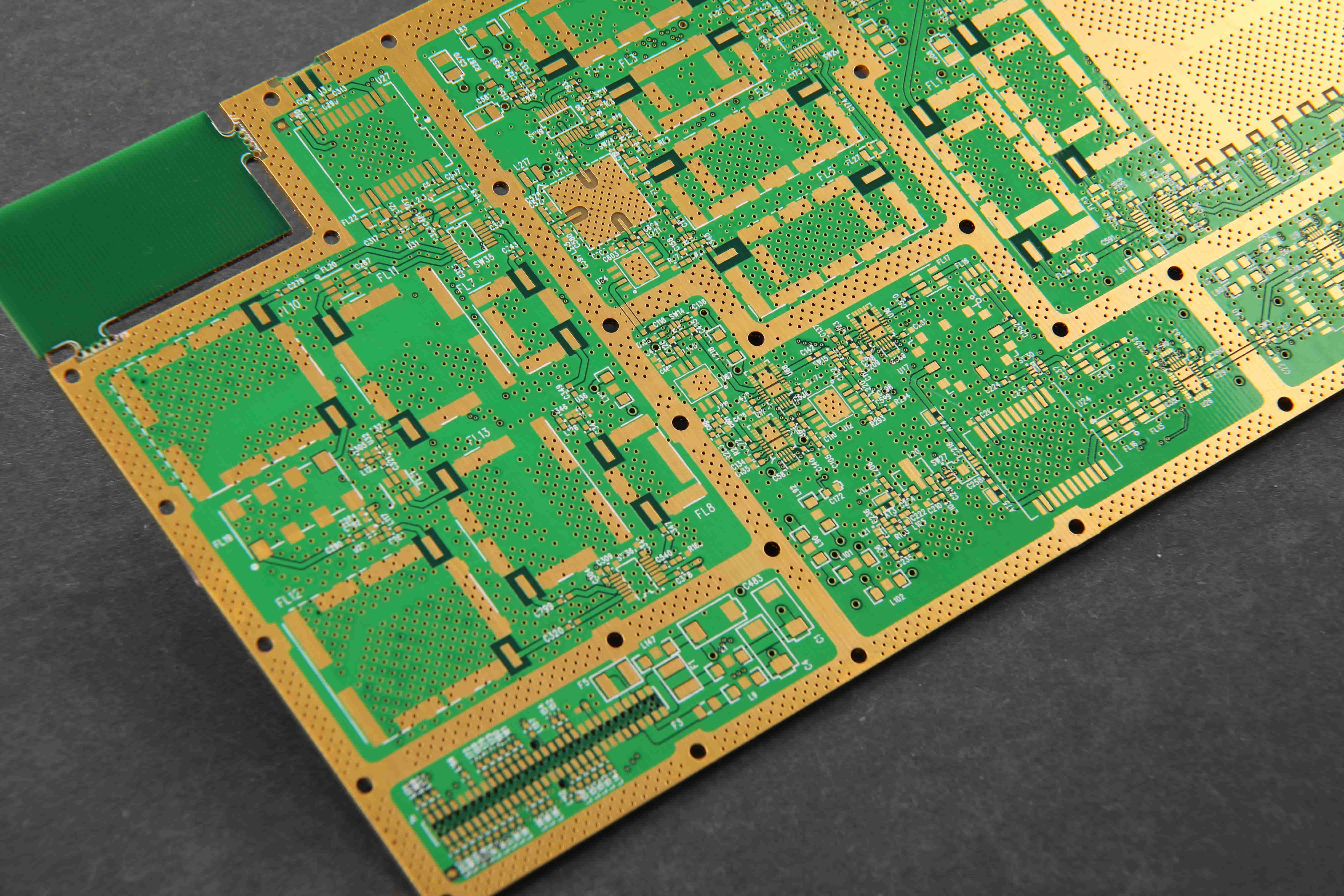
Heavy copper up to 11 OZ
0.00025” etch tolerance
+/- 5% controlled impedance
Unique Features
- Laminate thickness from 0.002” thin to 0.5” thick dielectric.
- Advanced Direct Imaging Machines for micro features and critical registration requirements.
- Mixed dielectrics and hybrid constructions in Multilayer configurations (3-22 layers).
- Hi speed Drilling & Routing with optics for optimized X,Y,Z Back Drilling, Controlled Depth Drilling, tight registration and tight tolerance control.
- Largest inventory of RF materials in North America from all domestic and international suppliers.
- Advanced tolerance Controlled Depth Routing with on-line depth measurements.
- Metal back PCBs.